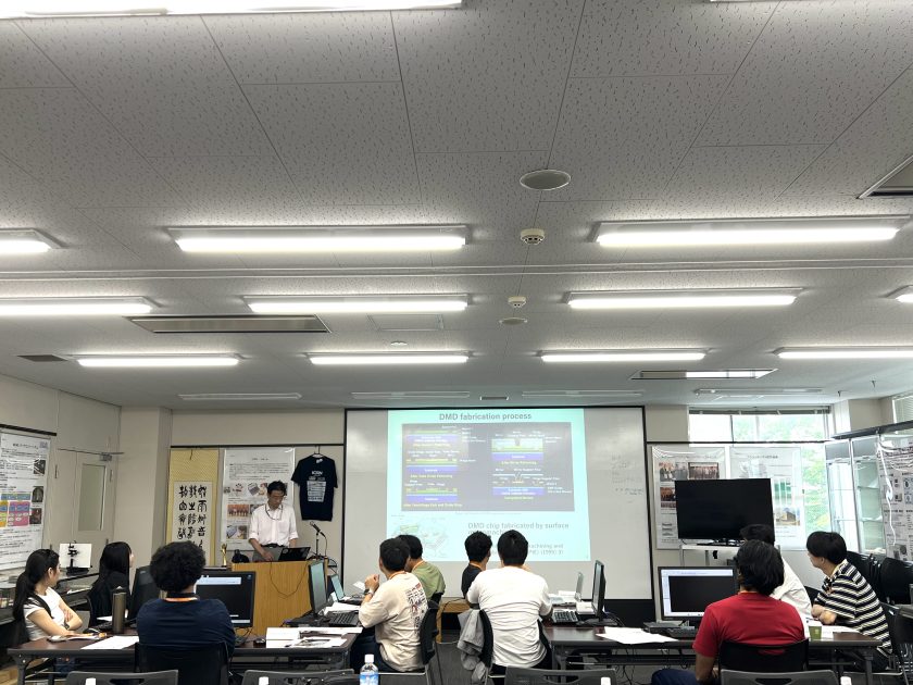
On July 31, 2026, ten students participating in the “UPWARDS for the Future Summer Program” visited the Micro System Integration Center at Tohoku University and took part in a hands-on semiconductor microfabrication training program.
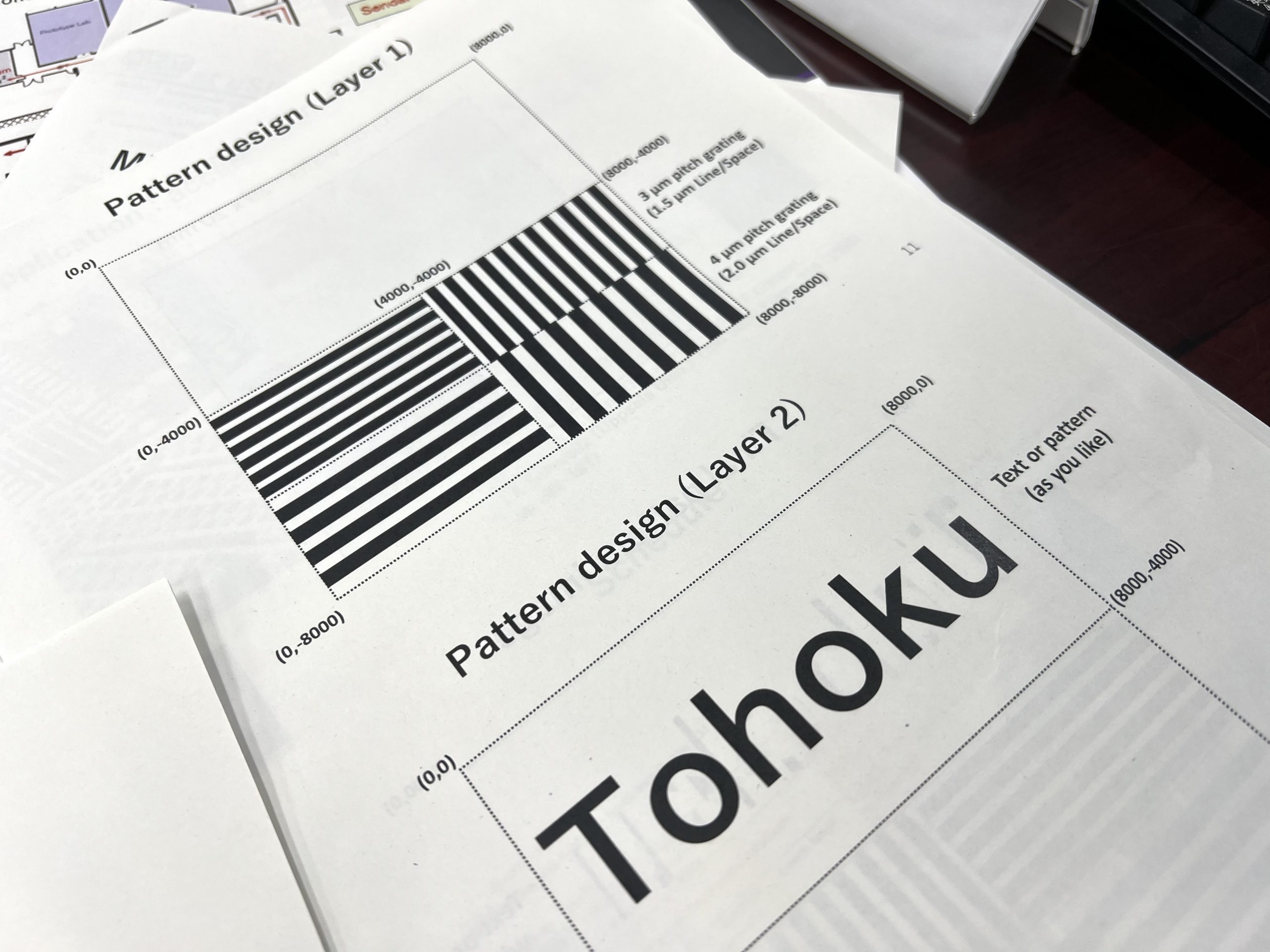
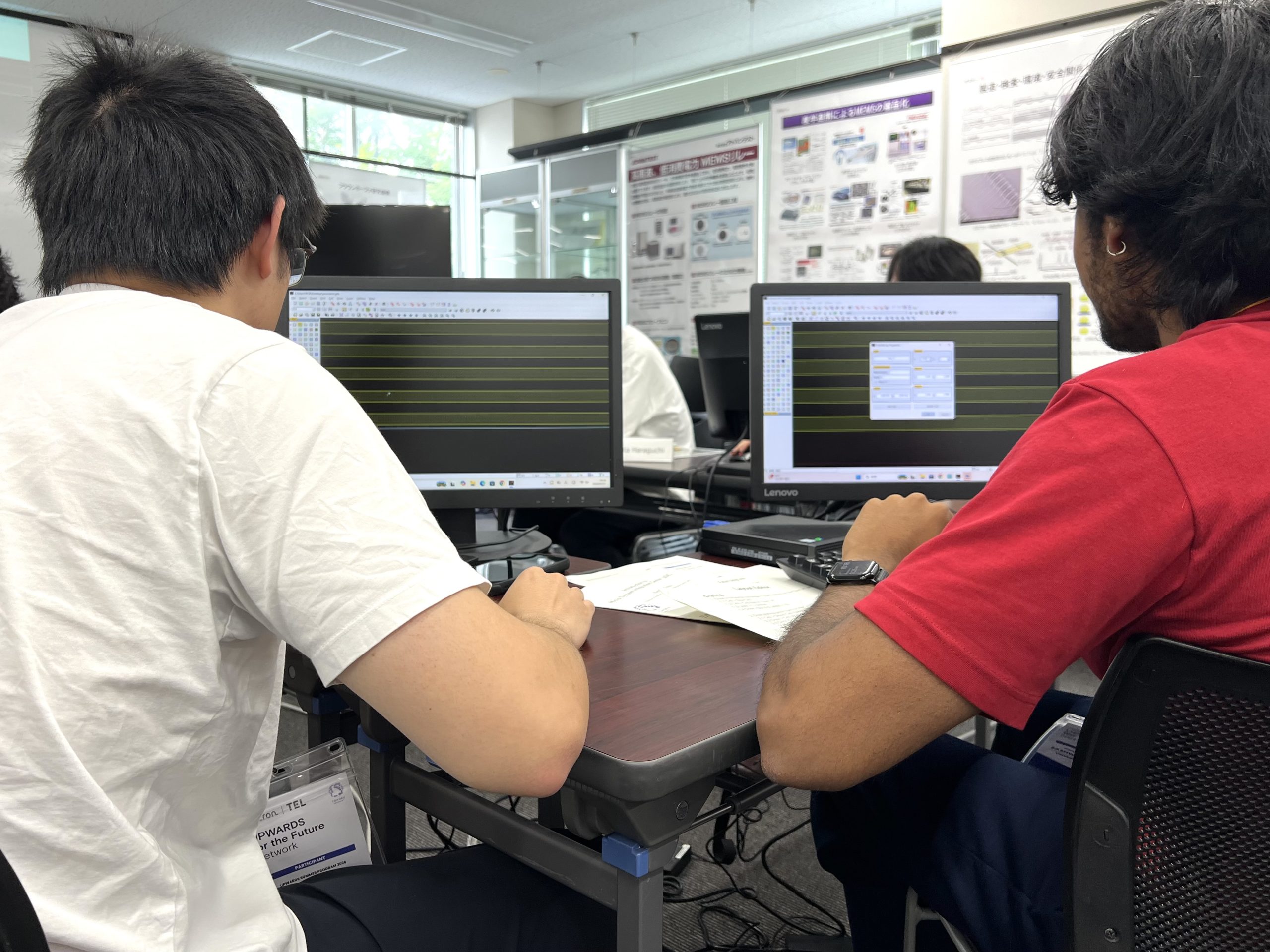
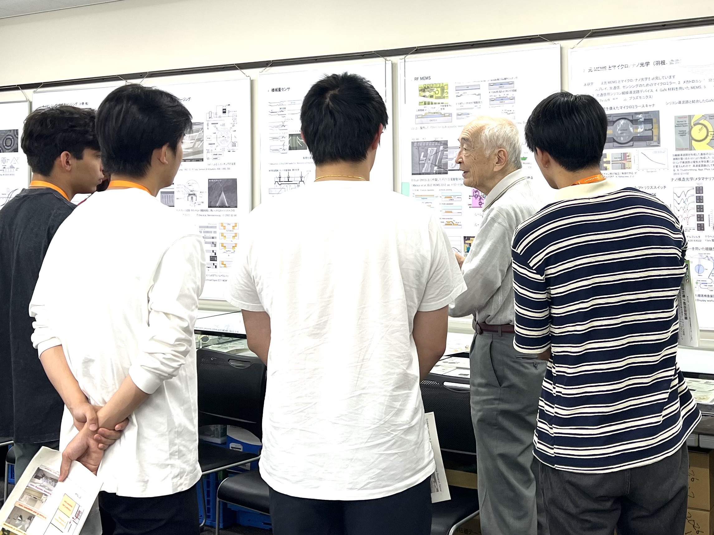
Following a lecture on the history and development of semiconductor research at Tohoku University, the students worked on designing line-and-space patterns using CAD software.
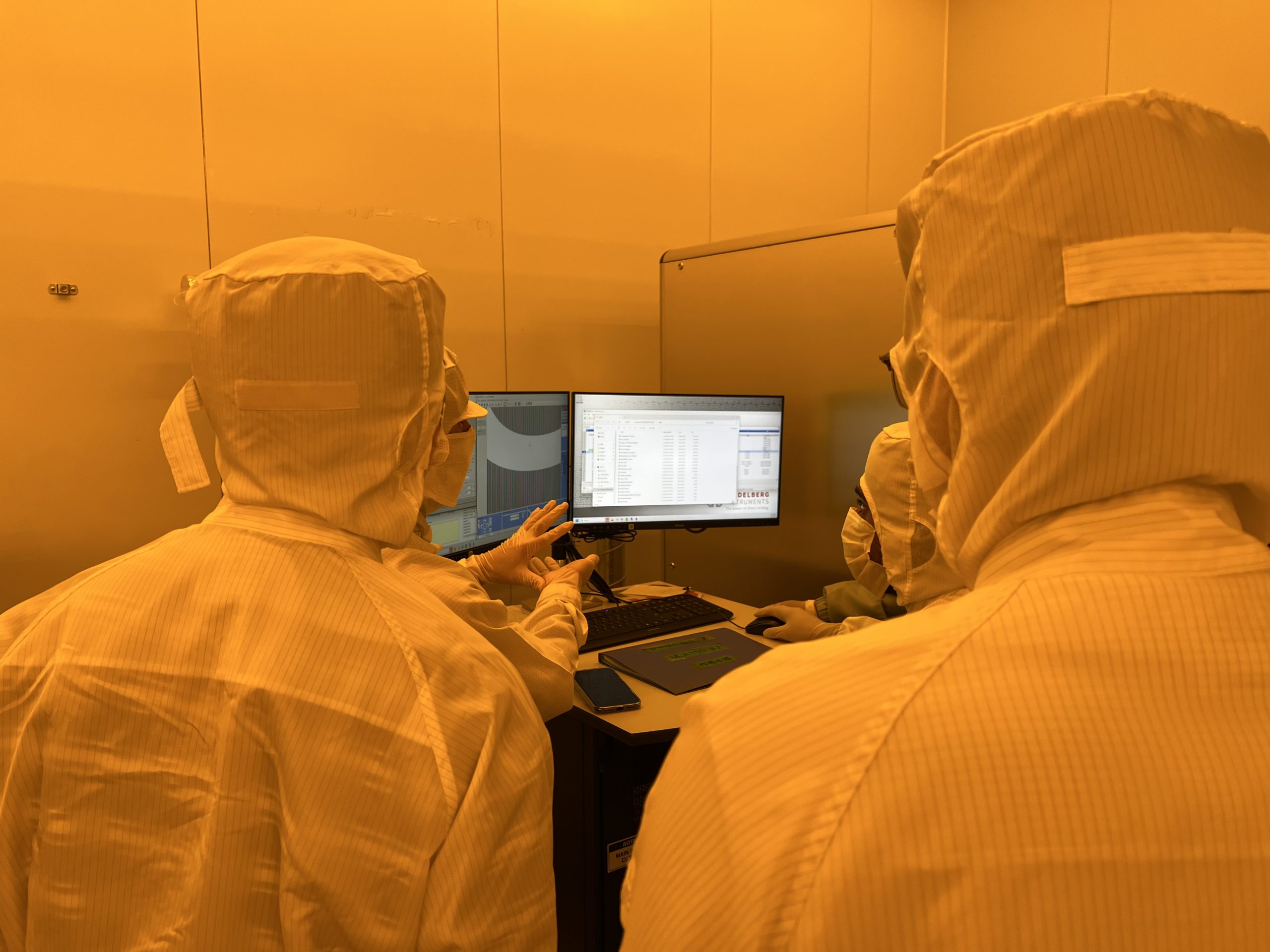
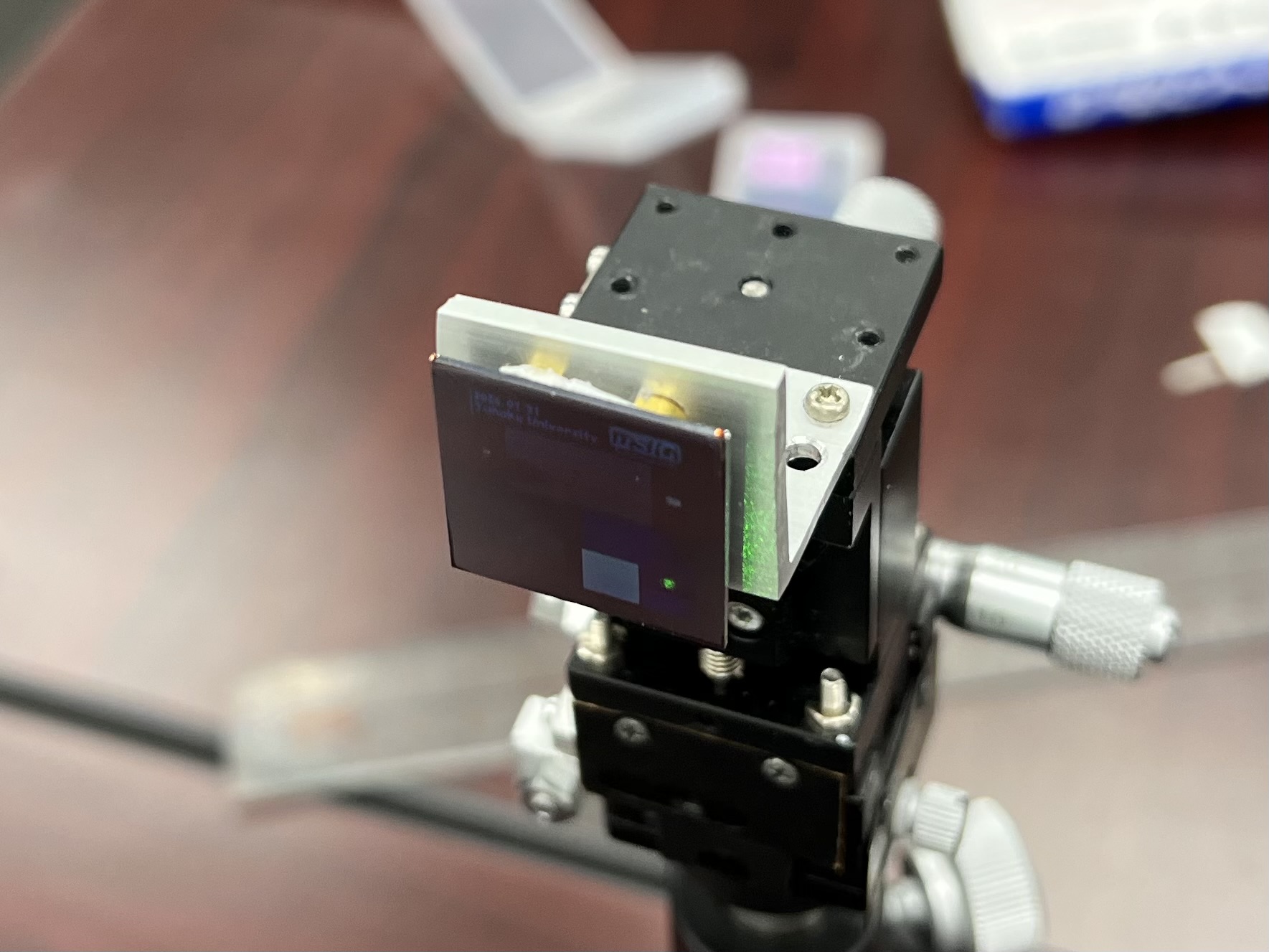
They then fabricated 20 mm square chips through a series of semiconductor manufacturing processes, including photoresist coating, pattern exposure using a maskless aligner, dry etching, and microscopic observation.
We hope that this hands-on training experience further sparked the participants’ interest in semiconductor technology and manufacturing.
2026年7月31日、「UPWARDS for the Future Summer Program」に参加する学生10名が、東北大学マイクロシステム融合研究開発センターを訪れ、半導体実習に参加しました。
東北大学における半導体研究の歴史や発展についての講義の後、設計ソフトを用いてライン&スペースパターンの作図に取り組みました。
その後、20mm角のシリコンウェハを用い、フォトレジスト塗布、マスクレスアライナを用いてのパターン描画、Deep-RIEのドライエッチングを行いました。
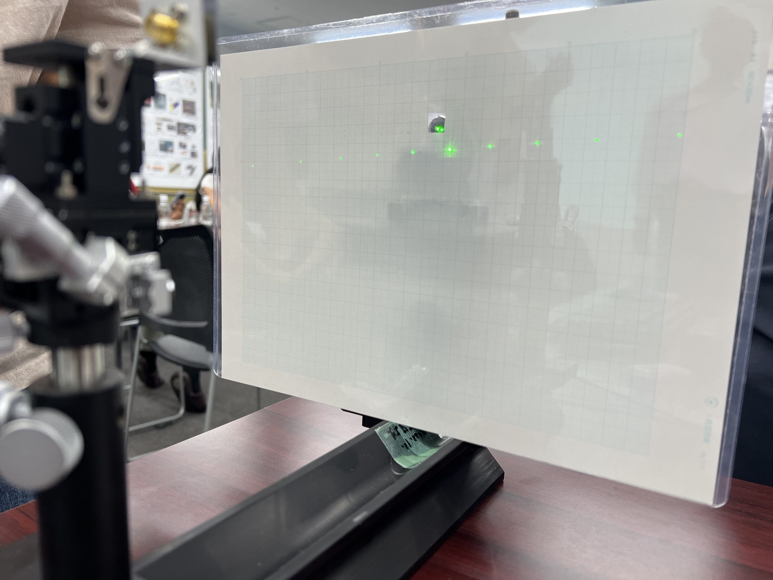
加工した後は、フォトリソグラフィによって形成された微細なパターンを顕微鏡で観察したほか、緑色レーザーをチップに照射し、微細構造によって光が広がる回折現象を観察しました。
今回の実習が、参加者の皆さんの半導体技術への興味を深める機会となれば幸いです。